
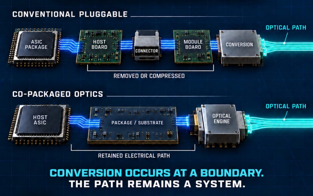
It shortens the electrical reach, tightens the integration and relocates the electro-optical boundary.
“Replacing electrons with photons” is a compelling way to describe the direction of co-packaged optics.
It is also incomplete.
CPO does not make electrical transport disappear. It changes the electrical distance to and from the conversion boundary—and where that boundary sits within the architecture.
That distinction matters.
Moving optics closer to switching or compute silicon can remove substantial electrical distance. It can reduce host-board reach, remove the electrical connector and module-board sections used by a conventional front-panel path, and reduce the associated loss and impedance discontinuities.
The result can be higher bandwidth density, lower power and less dependence on signal conditioning.
Those are real and important architectural advantages.
But the electrical path does not become zero.
It becomes shorter, more integrated and physically closer to the boundary where information passes between electrical and optical domains.
What the conventional path contains
In a conventional retimed pluggable architecture, data leaving an ASIC may cross several electrical regions before reaching the point of optical conversion:
- The ASIC’s on-die electrical I/O
- The die-to-package transition
- Package escape routing
- The package-to-board transition
- Host-board traces and layer transitions
- The connector footprint
- The electrical connector
- The module board
- The module’s signal-conditioning and conversion circuitry
Each region introduces its own physical conditions: impedance, loss, parasitics, reference behavior, coupling and manufacturing variation.
A retimed optical module places a regenerative boundary near the end of this electrical route. Its internal electronics recover and retransmit the signal before it is placed onto an optical carrier.
That architecture consumes power and introduces latency, but it also allows portions of the electrical and optical system to be designed, tested and qualified as more separable domains.
What CPO changes
Co-packaged optics moves the optical engine much closer to the host ASIC, typically onto the same first-level substrate.
Much of the conventional host-board reach can therefore be removed or compressed. The electrical faceplate connector and module-board path may also disappear from the high-speed electrical channel.
The path becomes dramatically shorter.
But several electrical regions remain:
- The ASIC’s electrical transmitter and receiver
- The die and package transitions
- Package-substrate, interposer or bridge routing
- The optical-engine attachment interface
- Electronic driver and receiver circuitry
- The interfaces connecting electronic and photonic devices
The precise arrangement varies.
The OIF Co-Packaging Framework Document considers re-timed, linear-amplified, half-retimed and direct-drive electrical interfaces. These architectures distribute signal conditioning differently, but each retains an electrical interface between the host ASIC and the optical engine.
On the transmit side, an electrical signal must reach the circuitry that drives the optical modulator.
On the receive side, the photodetector produces an electrical response that must be amplified, interpreted and delivered back to the host ASIC.
CPO therefore does not replace an electrical system with a purely optical one.
It brings the two physical regimes closer together and relocates the boundary between them.
A 50 mm path is still a path
The OIF framework makes the retained electrical channel explicit.
For its illustrative re-timed interface, the OIF describes approximately 50 mm of first-level packaging substrate, including package parasitics from the ASIC and optical-engine assemblies.
The document separately defines XSR as an electrical interface for approximately 50 mm of package-substrate distance, or 10 dB of channel loss at the Nyquist frequency of the baud rate.
These are informative architectural parameters, not evidence that CPO has a 10 dB problem.
They also do not suggest that the industry has overlooked the electrical path. Its inclusion in the framework confirms that it remains an engineered part of the system.
The narrower and more important conclusion is this:
A channel with physical length, package parasitics and finite loss has not been eliminated.
It has been relocated and engineered for a different environment.
The OIF’s architectural rationale is precise. Locating the optical engine close to the host ASIC allows high-speed electrical-channel losses and impedance discontinuities to be minimized.
Minimized—not eliminated.
Shorter does not mean unengineered
Length matters.
Reducing electrical reach can lower conductor and dielectric loss, reduce propagation delay and ease portions of the equalization burden.
That is one reason CPO is so consequential.
But length is not the only variable governing a high-speed electrical path.
The retained channel may still cross die attachments, bumps, package structures, substrate routing, engine attachments and electronic-photonic interfaces. Its behavior remains influenced by geometry, reference structures, parasitics, coupling, manufacturing tolerance and operating conditions.
Those effects are one part of a much broader CPO system challenge.
Thermal management, laser architecture, optical attachment, reliability, manufacturing yield, test access, serviceability and economics remain central to whether a CPO architecture can deliver sustainable system-level value.
The retained electrical path must be considered alongside those realities—not above them and not apart from them.
Shortening the path reduces impairments that increase with distance.
It does not remove the need to engineer the physical transitions that remain.
The boundary moves inside the architecture
With conventional pluggable optics, much of the electronic-photonic handoff is contained within a separable module at the faceplate.
With CPO, that handoff moves closer to the ASIC and becomes part of a more tightly integrated package environment.
This broadens the architectural question beyond whether an electrical channel reaches an optical engine and whether conversion occurs successfully.
The system increasingly brings several disciplines into the same physical region:
- High-speed electrical design
- Photonic integration
- Advanced packaging
- Thermal control
- Power delivery
- Optical attachment
- Manufacturing
- Test and reliability
Each discipline may be individually understood.
The more consequential question is how their interactions should be evaluated across the complete boundary.
Conversion occurs at a boundary. The path remains a system.
Electro-optical conversion is a physical process occurring at an interface within a larger transport path.
On the transmit side, an electrical signal reaches the driver. The driver excites a modulator, and the modulator places information onto an optical carrier.
In the opposite direction, a photodetector converts received optical energy into an electrical response. That response must then be amplified, interpreted and delivered back to the host.
But successful conversion alone does not define the useful performance of the complete system.
System performance also depends on what reaches the boundary, what emerges from it and how the surrounding architecture behaves under real electrical, thermal, manufacturing and operating conditions.
Conversion changes the physical carrier.
It does not remove the transport path surrounding it.
The question CPO makes more important
The industry does not need another argument about whether copper or optics will win.
Each physical regime creates value under different architectural conditions.
Electrical transport can provide high density and efficiency across short, controlled reaches. Optical transport can extend reach and bandwidth without the same distance-dependent electrical penalties.
CPO is powerful because it changes where the transition between those regimes occurs.
Once that boundary moves, a deeper question follows:
What must the complete system preserve as information approaches, crosses and leaves the point of conversion?
That is an architectural and measurement question.
At Mitas Electronics, we are examining where electrical and optical physics naturally belong as computing architectures scale—and what high-speed systems must preserve as transport moves across the boundaries between them.
The architecture comes before the technology.
And the boundary is part of the architecture.